Project Objectives
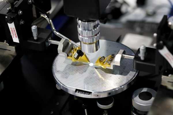
The project CHALLENGES – Real-time nano-CHAracterization reLatEd techNoloGiEeS – aims to develop innovative Non-Destructive Techniques (NDTs) for reliable inline multiscale measurements down to the nanoscale, and fully compatible with different factory environments. The developed metrology technologies will enable the increase of speed, resolution, sensitivity, spectral range and compatibility within different nano-related production environments, finally improving products performance, quality and reliability, with the consequent bosting of competitiveness. The CHALLENGES’s innovation will be developed exploiting the plasmonic enhancement of optical signals. It will provide a non-destructive approach based on the use of multipurpose nano-optical techniques to enable a reliable real-time nano-scale characterization in the factory floor, using plasmonic enhanced Raman, InfraRed (IR) and Photoluminescence signals.
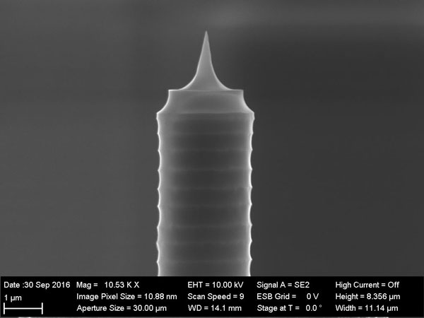
CHALLENGES is focused on broadening the scope of AFM techniques useable in semiconductor manufacturing by implementing suitable plasmonic-based technologies to bring in industrial environments the capabilities of optical spectroscopies at the nanoscale, already demonstrated at lab level. Such composite and hybrid measurement techniques will enable new applications for the already proven industrial AFM-based characterization technologies. Signal amplification by localized plasmon resonance at a sharp AFM tip will allow improving both the spatial resolution well beyond the optical diffraction limit and the local signal intensity with an improvement of the signal/noise ratio.
Improvements are also expected concerning the time scale resolving capabilities. The improvement of the spatial resolution will allow to obtain nanoscale spectral maps, compatible with the size of the current electronic devices, while the improved signal-to-noise ratio will allow for a faster and reliable punctual analysis.
The final goal is to develop nanoscale metrological NDTs based on SPM platforms, for doping, annealing, metal contamination, dangling bonds presence and strain measurement directly within the production lines with real-time capabilities.
Specific objectives of CHALLENGES are:
-
To provide a fully automated AFM-based tool
-
To develop large sample XY piezo scanning stages
-
To develop the optimum coupling solutions of light wavelengths range, AFM tip shapes and unconventional materials
-
To design and demonstrate a nanoscale metrological NDT system that is compatible with production lines that need cleanroom environment
-
To train a neural network capable to locate, with low-resolution hardware, relevant sites on the sample to probe with the high-resolution system, in a machine-learning framework
-
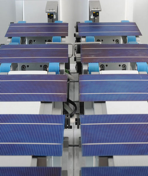
To demonstrate the process-adapted nanoscale metrology for the manufacturing industry, through its use in three relevant industrial application contexts related to CMOS electronics, Silicon Photovoltaics and 2D Materials


